
Learn about magnetoresistive random-access memory technology and what changes it brings for embedded products, including firmware updates and data logging.
Most embedded engineers know the limits of flash memory well. Writes are slow, and every write needs an erase first. Each cell survives only 10,000 to 100,000 write/erase cycles.
Magnetoresistive random-access memory (MRAM) removes most of these limits. It stores data as a magnetic state, not as trapped electrical charge. Microcontrollers built on 22 nm and 16 nm processes now use it, because embedded flash isn’t practical at those nodes.
This article explains how MRAM works, why flash stopped scaling, and what changes for firmware.
The Bit Is a Magnet, Not a Charge
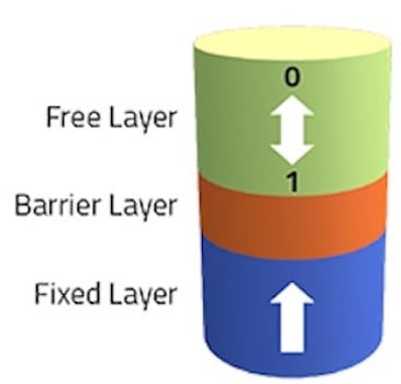
A flash cell stores a bit as electrons trapped on a floating gate or in a charge-trap layer. An MRAM cell stores it in a magnetic tunnel junction (MTJ). This is a stack of two ferromagnetic layers, usually a cobalt-iron-boron alloy (CoFeB), separated by a magnesium oxide (MgO) barrier about 1 nm thick.
As illustrated in Figure 1, one magnetic layer, the reference layer, has its magnetization fixed during manufacturing. The other is the free layer. Its magnetization can point in the same direction as the reference layer or the opposite direction. These two states are called parallel and antiparallel. This is a nonvolatile memory because both states are stable without power.
Figure 1. A basic implementation of a magnetic tunnel junction (MTJ) bit cell. Image used courtesy of Lam Research.
Reading relies on tunnel magnetoresistance (TMR). The barrier is thin enough for electrons to tunnel through, and they tunnel more easily when the two layers are parallel. The antiparallel orientation is typically two to three times higher resistance than the parallel orientation.
A sense amplifier compares the cell current against a reference and returns a 1 or a 0. That gap is small, which is why MRAM designs typically run error-correcting code (ECC) on every read.
Most embedded MRAM uses spin-transfer torque (STT) for the write operations. The write circuit drives a large current through the junction, and the electrons become spin-polarized as they pass through a magnetic layer. They carry that angular momentum into the free layer and set the magnetization direction. Reverse the current and the bit flips back. The bit cell is one access transistor and one MTJ, as shown in Figure 2.
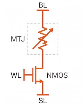
Figure 2. An MRAM cell consists of a magnetic tunnel junction (MTJ) bit cell in series with an NMOS transistor.
Flash Hits a 10 V Wall at 28 nm
Embedded flash scaling didn’t stall because the transistors became too small. It stalled due to voltage. The oxide for the flash memory must be roughly 8 nm to 10 nm thick, or the stored charge leaks away. Pushing electrons through oxide that thick takes about 10 V, but a 22 nm logic process runs its core below 1 V. Creating the 10 V on chip requires charge pumps and special high-voltage transistors, and neither shrinks with the rest of the logic.
Manufacturing makes it worse. Integrating a flash cell into a CMOS logic process adds 9 to 18 extra masks at 28 nm, according to figures reported by Semiconductor Engineering. The flash cell also does not integrate well with FinFET transistors. As a result, embedded flash is widely available down to 28 nm but rare below it.
MRAM avoids these problems:
- The MTJ sits between metal layers, above the transistors (Figure 3).
- MRAM works with planar, FD-SOI, and FinFET CMOS processes.
- MRAM needs only about three extra masks.
- The MRAM write voltage is close to normal logic levels.
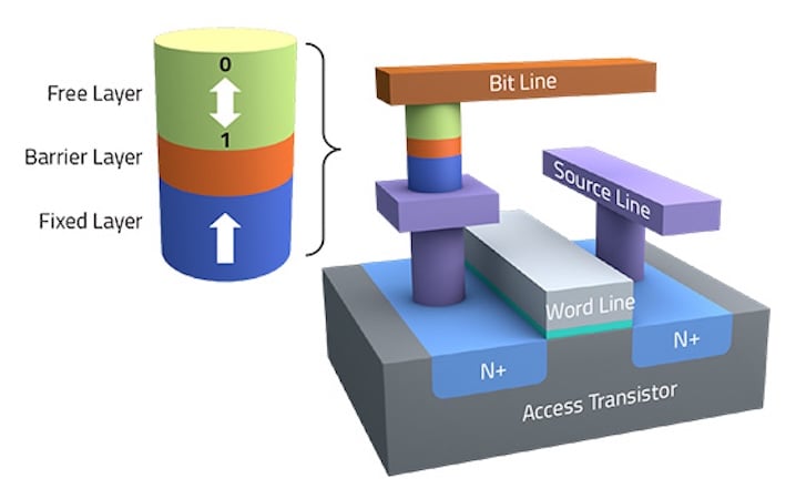
Figure 3. The MTJ bit cell integrates easily with the NMOS word line transistor. Image used courtesy of Lam Research.
Foundries now offer embedded MRAM at 28 nm, 22 nm, and 16 nm. For example, Renesas builds its RA8P1 microcontrollers on TSMC’s 22 nm process with up to 1 MB of MRAM. NXP has announced that its S32K5 automotive microcontrollers use MRAM on a 16 nm FinFET process.
Is MRAM Endurance Really Infinite?
One limitation of Flash memory is that it wears out. Each program and erase forces charge through the oxide. The oxide accumulates damage until it can no longer hold charge adequately.
MRAM switching moves no atoms and stores no charge, so the magnetic layers themselves do not wear out. That is how Everspin’s EMxxxLX Industrial STT-MRAM can specify unlimited read, write, and erase operations for the supported life of the product. Those devices also support 10 years of retention as a minimum.
TSMC specifies one million cycles for its 16 nm embedded MRAM. The write current stresses the thin MgO barrier, so designers of embedded memory must trade endurance against retention at high temperature. TSMC’s 16 nm FinFET MRAM is therefore specified for one million cycles with 20-year retention at 150°C. This is still 10 times the endurance of flash.
MRAM is also faster than flash. TSMC reports average write pulses slightly over 30 ns and 6 ns read times for a 22 nm design tuned for speed. And there is no erase step. NXP says its 16 nm MRAM can update 20 MB of code in about 3 seconds, a job that takes flash about 1 minute.
Table 1 compares STT-MRAM with NOR flash.
Table 1. Typical characteristics of embedded NOR flash and STT-MRAM.
| Characteristic | Embedded NOR Flash | STT-MRAM |
| Storage mechanism | Trapped electrical charge | Magnetization direction of the free layer |
| Erase before write | Yes, by sector | No |
| Write time | Microseconds to program; milliseconds to erase a sector | About 30 ns write pulse |
| Write voltage | About 10 V or more, from charge pumps | Close to logic supply levels |
| Endurance | 104 to 105 cycles | 106 to unlimited cycles |
| Data retention | Typically 10 to 20 years | Typically 10 to 20 years |
| Extra masks | 9 to 18 at 28 nm | About 3 |
| Main sensitivities | Oxide wear, charge leakage | Strong magnetic fields, high temperature |
Your Firmware Gets Simpler, With Three New Checks
Think about what your flash driver does today. It erases a whole sector, waits, and then programs it page by page. An MRAM driver simply overwrites data in place, and it can change a single word without needing to erase and rewrite its neighbors. Therefore, over-the-air updates finish faster, so your device spends less time half-updated. Production-line programming speeds up too.
Data logging benefits even more. With flash, your firmware buffers records in RAM, manages sector erases, and spreads writes with wear leveling. A power failure during a long erase can still corrupt data.
With MRAM, each record goes straight to its final address in microseconds. The reduced time means a corresponding reduction in the likelihood of losing data due to a power failure.
Don’t Skip the Math
While 1 million write/erase cycles sounds like a lot, don’t skip the math when designing your application. Imagine an energy meter that saves its running total once per second. If you write to one fixed address in an embedded MRAM, you will exceed 1 million cycles in under 12 days.
If you design your code to rotate across 1,000 different addresses, then the same memory lasts about 32 years. If you are writing only once an hour, a million cycles would allow your MRAM to operate for more than 100 years.
Three MRAM Questions
Before you commit to an MRAM design, you should make three datasheet checks that flash never asked of you:
- Magnetic immunity
- Retention at temperature
- Solder reflow characteristics
Let’s take a look at magnetic immunity first. A strong external field can disturb an MTJ, so vendors specify a maximum. TSMC reports ten-year immunity above 1,100 Oe at 25°C for its 22 nm MRAM. Compare the rating with any motors, magnets, or large inductors near your board.
Second, examine the retention specs at your maximum operating temperature, not at room temperature.
Third, solder reflow. If you program parts before assembly, the data must survive the reflow oven. TSMC’s 22 nm MRAM retains data through six reflow cycles, but its speed-tuned variant gives up that capability.
If your part passes all three and your write rates fit its endurance, MRAM is the simpler memory to design with. Below 28 nm, embedded flash will rarely be on the menu anyway.
Summary
MRAM stores data as a magnetic state, so it avoids the high voltages and extra masks that stopped embedded flash at 28 nm. It writes fast, needs no erase step, and has far higher endurance than flash. Before you pick a part, check its endurance, magnetic immunity, retention at temperature, and solder reflow rating.