This project brief describes how to build a compact, high-current half-bridge module that drives two N-channel MOSFETs for automotive and other high-power switching applications.
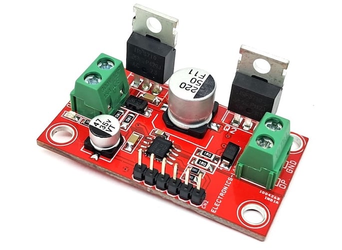
The Automotive Half-Bridge Driver is a small module for switching loads of up to 36 V DC. It is built around the UCC27211A-Q1, a 120 V half-bridge gate driver, and two IRF3710 power MOSFETs. The driver sources 3.7 A and sinks 4.5 A, so it can switch large MOSFETs quickly and keep switching losses low (Figure 1).
The two gate-driver inputs are independent. A microcontroller or PWM controller can control the high-side and low-side MOSFETs separately. An integrated bootstrap diode supplies the high-side gate drive, so no external bootstrap diode is needed. A red LED shows when the gate-driver supply is present.
Figure 1. The assembled Automotive Half-Bridge Driver module.
Specs and Features
- Load supply: 36 V DC (limited by the DC bus capacitor rating)
- Gate driver supply: 12 V to 15 V DC (operating range 8 V to 17 V)
- Drives two N-channel MOSFETs in a high-side and low-side configuration with independent inputs
- Maximum bootstrap voltage: 120 V DC
- Output current: 3.7 A source and 4.5 A sink
- Input pins tolerate –10 V to +20 V, independent of the supply voltage
- TTL-compatible inputs
- Rise time of 7.2 ns and fall time of 5.5 ns with a 1000 pF load
- Typical propagation delay of 20 ns, with 4 ns delay matching
- Symmetrical undervoltage lockout (UVLO) for the high-side and low-side drivers
- Power LED indicator
- PCB dimensions: 50.80 mm × 27.94 mm
How It Works
The UCC27211A-Q1 is a high-side and low-side gate driver with a peak output of 3.7 A source and 4.5 A sink. This strong drive moves the MOSFET gates quickly through the Miller plateau, which reduces switching losses. Figure 2 shows how the driver connects to a PWM controller and a half-bridge power stage.
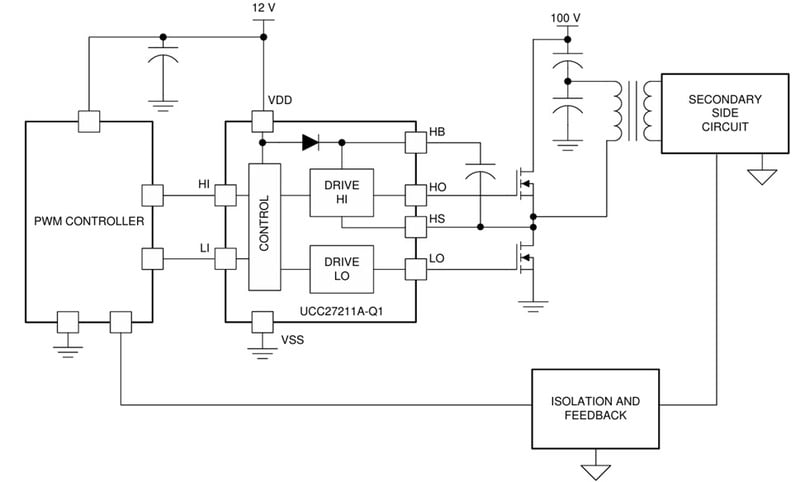
Figure 2. Typical application circuit of the UCC27211A-Q1. Image courtesy of Texas Instruments.
The inputs tolerate –10 V directly, so they can connect to a gate-drive transformer without rectification diodes. They are also independent of the supply voltage and accept up to 20 V. The TTL-compatible inputs have enhanced hysteresis, which improves noise immunity with analog and digital PWM controllers. The switching node (HS pin) tolerates voltages down to –(24 – VDD) V. This protects the high-side driver from negative transients caused by parasitic inductance and stray capacitance.
The two drivers are precisely matched. The typical propagation delay difference is only 4 ns on both turn-on and turn-off. An integrated 120 V bootstrap diode removes the need for an external one. The UVLO protection covers both drivers. It forces the outputs low whenever the drive voltage falls below the threshold, so turn-on and turn-off behave symmetrically.
MOSFETs
The module uses two IRF3710 MOSFETs. The IRF3710 is a 100 V N-channel HEXFET power MOSFET. It handles a continuous drain current of up to 57 A and has an on-resistance of about 23 mΩ. This makes it suited to DC-DC converters, motor drivers, inverters, and UPS systems.
You can replace the MOSFETs with other devices to match your voltage, current, and switching frequency. The gate driver supports applications up to 100 V. If you change the MOSFETs, adjust the gate resistors and the bootstrap capacitor to suit the new gate capacitance and switching frequency.
Schematic and Bill of Materials
Figure 3 shows the schematic. The input signals pass through 47 Ω resistors (R3 and R5) to the HI and LI pins of U1. Each MOSFET gate has a 1 Ω resistor, and a second 1 Ω resistor with an SS34 diode forms a separate turn-off path (R2/R4/D2 for Q1 and R6/R7/D3 for Q2). C5 is the bootstrap capacitor. C3 and C4 decouple the load supply.
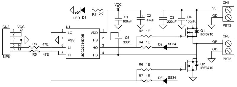
Figure 3. Schematic of the Automotive Half-Bridge Driver.
The bill of materials is shown in Table 1.
Table 1. BOM for the Automotive Half-Bridge Driver.
| REF | DESCRIPTION | QTY | MFG | SUPPLIER | PART NO. |
| CN1, CN3 | 2-pin screw terminal, 2.54 mm pitch | 2 | Phoenix | DigiKey | 277-1247-ND |
| CN2 | 6-pin male header, 2.54 mm pitch | 1 | Würth | DigiKey | 732-5319-ND |
| C1 | 100 nF / 50 V ceramic, SMD 0805 | 1 | Yageo/Murata | DigiKey | |
| C2 | 47 µF / 35 V electrolytic | 1 | Würth | DigiKey | 732-8419-1-ND |
| C3 | 220 µF / 50 V electrolytic | 1 | Nichicon | DigiKey | 493-6390-1-ND |
| C4 | 100 nF / 100 V ceramic, SMD 1206 | 1 | Yageo/Murata | DigiKey | |
| C5 | 330 nF / 35 V ceramic, SMD 1206 | 1 | Yageo/Murata | DigiKey | |
| D1 | Red LED, SMD 0805 | 1 | OSRAM | DigiKey | 475-1278-1-ND |
| D2, D3 | SS34 Schottky diode, SMD | 2 | Taiwan Semi | DigiKey | 1801-SS34LCT-ND |
| Q1, Q2 | IRF3710 MOSFET, TO-220 | 2 | Infineon | DigiKey | IRF3710PBF-ND |
| R1 | 2 kΩ, 5%, SMD 0805 | 1 | Yageo/Murata | DigiKey | |
| R2, R4, R6, R7 | 1 Ω, 5%, SMD 1206 | 4 | Yageo/Murata | DigiKey | |
| R3, R5 | 47 Ω, 5%, SMD 0805 | 2 | Yageo/Murata | DigiKey | |
| U1 | UCC27211DDR gate driver | 1 | TI | DigiKey | 296-30344-1-ND |
Connections
Figure 4 shows the connectors and their labels.
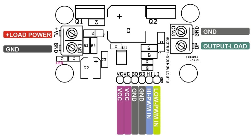
Figure 4. Connection diagram for the Automotive Half-Bridge Driver.
CN1 — Load Supply (2-pin screw terminal):
- Pin 1 = +Load Supply (+VL)
- Pin 2 = GND
CN2 — Control Header (6-pin, 2.54 mm pitch):
- Pins 1 and 2 = VCC (gate driver supply, 12 V to 15 V)
- Pins 3 and 4 = GND
- Pin 5 = High-Side PWM Input (HI)
- Pin 6 = Low-Side PWM Input (LI)
CN3 — Output (2-pin screw terminal):
- OP = Output to the load (switching node)
- GND = Ground
D1 — Power LED:
- Lights when the gate driver supply is present
PCB Files
Figure 5 shows the silkscreen, top layer, and bottom layer of the 50.80 mm × 27.94 mm PCB.
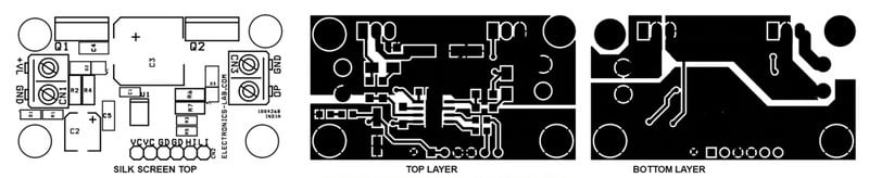
Figure 5. PCB layout of the Automotive Half-Bridge Driver: silkscreen, top layer, and bottom layer.
You can download the layout files for this project here:
Except where noted, all images used courtesy of Rajkumar Sharma